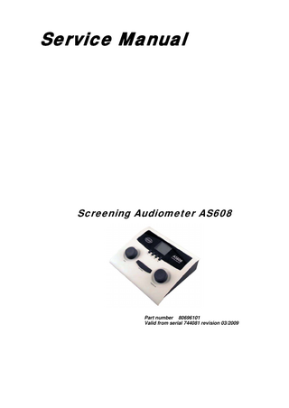
Service Manual
26 Pages
Preview
Page 1
Service Manual
Screening Audiometer AS608
Part number 80696101 Valid from serial 744081 revision 03/2009
Contents Contents ... 1 General Technical Specifications ... 2 Frequencies and maximum intensities ... 2 Specification of input/output connections ... 3 Calibration properties ... 3 Survey of reference values for pure tone audiometer calibration ... 3 General properties for earphones ... 4 Accessories ... 5 Consumables ... 5 Spare parts ... 6 Disassembly ... 7 Change batteries ... 7 Open instrument ... 8 Wire connections ... 9 Schematics ... 10 Analog Block Diagram ... 10 Main board Diagram ... 11 Component Index Top ... 16 Component index bottom ... 17 Component Part List ... 18 Calibration Procedure ... 21 Service, adjustment and repair... 21 Equipment for Calibration... 21 Calibration mode entering ... 21 Attenuator Calibration ... 22 Headset Calibration ... 23 Attenuator Calibration (Alternative performed without disassembly) ... 24 Update News Appendix U ... 25
AS608 Service Manual Page 1
General Technical Specifications
Standards:
The CE-mark indicates that Interacoustics A/S meets the requirements of Annex II of the Medical Device Directive 93/42/EEC. Approval of the quality system is made by TÜV - identification no. 0123. IEC 60601-1, Class I, Type B Safety: (using external power supply or batteries) IEC 60601-1-2 EMC: IEC 60645-1/ANSI S3.6 , Type 4 Tone audiometer Audiometer:
Power:
Batteries:
Medical CE-mark:
Temperature:
3 AA size Battery life: stand by: 6 months Tone presentations: 70.000 Automatic battery on/off switching Automatic battery status indicator External power supply ASA30M, Input: 100-240 VAC, 0.8-0.4 A, 47-63 Hz Output: 5 VDC – 4.0A 15 – 35 °C
Rel. Humidity:
30 – 90%
Optional:
Operation environment:
Storing/handling:
Temperatures below 0°C and above 50°C may cause permanent damage on the instrument and its accessories.
Functions Signal sources:
Tone:
Inputs:
Pat. Response
Outputs: Attenuator: Tone Switch: Tone presentation:
Power ASA30M Earphone Right / Left:
Manual: Reverse: Pulse:
11 pure tone and warble test frequencies in the range of 125 – 8000Hz Connection for patient response switch. Response is shown in display (Optional) Connection for external power supply via USB standard earphones -10 to 100 dB in 5 dB steps. Switch for presentation of signals. Indicated in display when activated Tone is presented by activation of Tone Switch. Can be selected in setup menu Automatic pulsing width selectable 250 or 500ms in setup menu
Frequencies and maximum intensities Frequency
Air Conduction TDH39
Frequency
Air Conduction TDH39
Hz
dB HL
Hz
dB HL
125 250 500 750 1000
70 90 100 100 100
1500 2000 3000 4000 6000 8000
100 100 100 100 100 90
AS608 Service Manual Page 2
Specification of input/output connections Inputs Power USB 1.1 comm. Patient response
Connector type USB plug USB plug Jack, 6.3mm stereo
Outputs: Phones, Left/ Right Jack, 6.3mm mono
Electrical properties 5V 90Ω Impedance Accepts both mono and stereo 6.3mm jack Uses sleeve + tip or ring + tip for response. Tip 3.3V through 1KΩ. Impedance total 6,75KΩ for stereo, 6,25KΩ for mono.
Voltage: Min. load impedance: Output impedance: Connection:
Up to 3V rms. by 10Ω load 5Ω 0,5Ω Uses sleeve + tip mono 6.3mm jack.
Other electrical specifications: Warble 5 Hz sine, ±5% modulation
Calibration properties Telephonics TDH39 with a static force of 4.5N ±0.5N
Calibrated Transducers:
Earphones:
Accuracies:
Generally the instrument is made and calibrated to be within and better than the tolerances required in the specified audiometer standards: Frequency: ±2% Pure tone levels: ±3 dB for 125 – 4000Hz ±5 dB for 6000 – 8000Hz
Tone calibration standards and spectral properties: Earphones Pure tone: ISO 389-1/ ANSI S3.6 for TDH39.
Survey of reference values for pure tone audiometer calibration Freq.
[Hz] 125 250 500 750 1000 1500 2000 3000 4000 6000 8000
ISO 389-1
ANSI S3.6
(TDH39) [dB re. 20 µPa] 45.0 25.5 11.5 7.5 7 6.5 9 10 9.5 15.5 13
(TDH39) [dB re. 20 µPa] 45 25.5 11.5 8 7 6.5 9 10 9.5 15.5 13
AS608 Service Manual Page 3
Coupler types used by calibration: − −
TDH39 is calibrated using a 6cc acoustic coupler made in accordance to IEC 303 Insert phones are calibrated using a 2cc acoustic coupler made in accordance to IEC 126
General properties for earphones Sound attenuation values for earphones Frequency
[Hz] 125 160 200 250 315 400 500 630 750 800 1000 1250
Attenuation TDH39 with MX41/AR or PN 51 cushion [dB] 3 4 5 5 5 6 7 9 11 15 18
Frequency
[Hz] 1500 1600 2000 2500 3000 3150 4000 5000 6000 6300 8000
Attenuation TDH39 with MX41/AR or PN 51 cushion [dB] 21 26 28 31 32 29 26 24
General about Specifications Interacoustics continuously strive to improve the products and their performance. Therefore the specifications can be subject to change without notice. The performance and specifications of the instrument can only be guarantied if it is subject to a technical maintenance at least once a year. This should be made by a workshop, authorised by Interacoustics. Questions about representatives and products may be sent to: Interacoustics A/S Phone: +45 63713555 Drejervaenget 8 Fax: +45 63713522 DK 5610 Assens email: [email protected] Denmark http: www.interacoustics.com
AS608 Service Manual Page 4
Accessories
Item
# IA Item Number
Description
80000101
TDH39 Audiometric Headset 30° plug
37302101
IEC-M31 Earphone cord
80000201
TDH39P with Peltor
80041201
50250 Peltor noise enclosures
76401301
TDH-39P 10 Ohm Earphone Telephonics
80041001
MX41 Cushion Mod 51
# IA Item Number
Description
81401402
Pen set
81410002
Audiogram chart AF12
80406301
Batteriy 1,5Volt LR6 14,5x50,5m
Consumables Item
(position 20 on index page 8)
AS608 Service Manual Page 5
Spare parts Item
# IA Item Number
Description
Index on assembly sketch
34710201
Cabinet top 096 – display glass enclosed
1+6
34710303
Cabinet bottom 096
2
34710501
Bracket display 096
9
76103901
Display LCD 128x64 dots
12
34117002
Button large 096
4
34116902
Button small 096
3
34815401
Damper
21
36309902
Button rotary complete
10
34710401
Cover battery 096
8
51016406
PCA Main board assembled
11
75002301
Jack 6.3mm Stereo + SW gold right angle
AS608 Service Manual Page 6
Disassembly Change batteries Turn instrument upside down. Dismount the battery cover and replace the batteries.
Index shows IA item numbers – referring to spare part list on page 6 20
8
AS608 Service Manual Page 7
Open instrument To open the cabinet, turn the instrument upside down, and remove 5 screws pos 18. Index shows IA item numbers – referring to spare part list on page 6
AS608 Service Manual Page 8
Wire connections
BRN
RED
BRN
RED
Display connections
2xBRN
2xRED
RED
RED
BRN
BRN
Battery terminals connection
AS608 Service Manual Page 9
3V3
Vbat ANA ON
+5V -5V
SMPS
Vref
USB
Vatt DAC L/R Keyboard Rotary
Power Select
USB
TF
MUTE
HOLD
MCU
Vbat
SPI
V DIST
-10dB
TF
-10dB
I2C
LEFT CODEC
I2S
3V3
3V3 SMPS
ANA ON
Att.
-10dB
THAT2181
DG419
Power DG419
BAT
3V3
OUTPUT
RIGHT L/R
MUTE
1V8 REG
GND
DISPLAY TF MIC SHDN
3V3
Pat Resp Switch
Date
Constr.
Appr.
030708
PSC
OG
Sheet
Revision 101208
PSC
EN
1 of 1
Constr.
Title
Block Diagram 096 Partno.
-
Drawingno.
NP = Not Present
D02022802
AS608 Service Manual Page 10
MCU - LPC2368FB100
VUSB_+5V SDI_DISP RS_DISP CS#_FLASH
Page2 Page2
SCK_DAC CS#_DAC DO_FLASH SDI_DAC C-SW1-A C-SW1-B TONE PAT-RESP CODEC_BCLK
Page2 Page5 Page5 Page4 Page4
R11 R16
+3.3V_CPU +3.3V_CPU
R95 R96 R97 R98 R99 R100 R101
DGND DGND DGND DGND DGND DGND DGND
4K75 4K75
10K5 4K75 10K5 10K5 10K5 10K5 10K5
CODEC_WCLK CODEC_DOUT P0.26 PA16 CODEC_SDA CODEC_SCL
CODEC_SDA CODEC_SCL
POWER_HOLD ANALOG_ON MUTE# LEFT/RIGHT 10dB TF BL-ON LED1 NP
R6
+3.3V_CPU
Page3 Page3
USBD+ USBD-
Page4 Page3 Page2 Page2 Page2 Page2 Page3
POWER_HOLD ANALOG_ON MUTE# LEFT/RIGHT 10dB TF BL-ON P1.15 PA17
Page4
KEY_DOWN P1.17 PA18
NP Page3
HSMG-C190
CODEC_RESET# P1.20 PA6 P1.21 PA3 P1.22 PA1 P1.23 PA8
Page4 Page4 Page4 Page4,5 Page4,5 R1
DGND
10K5
VUSB_+5V
KEY_0 KEY_1 KEY_2 KEY_3 KEY_4 P1.29 PA9 VUSB_+5V VBAT_MON
Page3
P2.0 P2.1 P2.2 P2.3 P2.4 P2.5 P2.6 P2.7 +3.3V_CPU
R73
4K75
+3.3V_CPU
R45
10K5
USB_ACT
CODEC_BCLK CODEC_WCLK CODEC_DIN
P2.10
XTAL2
23
77 76 48 49
P0[8]/I2STX_WS/MISO1/MAT2[2] P0[9]/I2STX_SDA/MOSI1/MAT2[3] P0[10]/TXD2/SDA2/MAT3[0] P0[11]/RXD2/SCL2/MAT3[1]
R63 R62 R104 R57 R52 R50 R49 R44 R66
22 22 22 22 22 22 22 22 22
62 63 61 60 59 58 57 56 9
P0[15]/TXD1/SCK0/SCK P0[16]/RXD1/SSEL0/SSEL P0[17]/CTS1/MISO0/MISO P0[18]/DCD1/MOSI0/MOSI P0[19]/DSR1/MCICLK/SDA1 P0[20]/DTR1/MCICMD/SCL1 P0[21]/RI1/MCIPWR/RD1 P0[22]/RTS1/MCIDAT0/TD1 P0[23]/AD0[0]/I2SRX_CLK/CAP3[0]
R71 R72
22 22
R23 R24
22 22
8 7 6 25 24
P0[24]/AD0[1]/I2SRX_WS/CAP3[1] P0[25]/AD0[2]/I2SRX_SDA/TXD3 P0[26]/AD0[3]/AOUT/RXD3 P0[27]/SDA0 P0[28]/SCL0
R41 R25
22 22
29 30
P0[29]/USB_D+ P0[30]/USB_D-
R81 R82 R83 R84 R85 R86 R87
22 22 22 22 22 22 22
95 94 93 92 91 90 89 88
P1[0]/ENET_TXD0 P1[1]/ENET_TXD1 P1[4]/ENET_TX_EN P1[8]/ENET_CRS P1[9]/ENET_RXD0 P1[10]/ENET_RXD1 P1[14]/ENET_RX_ER P1[15]/ENET_REF_CLK
R102 R26
22 22
R27 R20 R28 R17 R29
22 22 22 22 22
R48 R39
22 22
R68
22
R42 R43 R30
22 22 22
RTCX1
16
RTCX2
18
RESET
RSTOUT
75 74 73 70 69 68 67 66
P2[0]/PWM1[1]/TXD1/TRACECLK P2[1]/PWM1[2]/RXD1/PIPESTAT0 P2[2]/PWM1[3]/CTS1/PIPESTAT1 P2[3]/PWM1[4]/DCD1/PIPESTAT2 P2[4]/PWM1[5]/DSR1/TRACESYNC P2[5]/PWM1[6]/DTR1/TRACEPKT0 P2[6]/PCAP1[0]/RI1/TRACEPKT1 P2[7]/RD2/RTS1/TRACEPKT2
65 64 53 52 51 50
P2[8]/TD2/TXD2/TRACEPKT3 P2[9]/USB_CONNECT/RXD2/EXTIN0 P2[10]/EINT0 P2[11]/EINT1/MCIDAT1/I2STX_CLK P2[12]/EINT2/MCIDAT2/I2STX_WS P2[13]/EINT3/MCIDAT3/I2STX_SDA
PA20 PA19
82 85
P4[28]/MAT2[0]/TXD3 P4[29]/MAT2[1]/RXD3
VDDA
R15 1M C6
R54
100K 22
DGND
RESET#
+3.3VA
TP10 TP9 TP8 TP7 TP5
TRST# TDI TMS TCK TDO Page3,5
Page3,4 POWER_ON
2
1 3 5 7 9 11 13 15 17 19
TRST# TDI TMS TCK RTCK TDO RESET#
1
D3 BAS40-02V
2 4 6 8 10 12 14 16 18 20
R13 10K5
CODEC_MCLK
R10 1M
Page3,5
+3.3VA
14
R60
22
RSTOUT# NP
C1 22p 5% NP0
GND
VDD(DCDC)(3V3) VDD(DCDC)(3V3) VDD(DCDC)(3V3)
12
R56
22
+3.3V
R61
NP
Vref
10
Page2,3
DGND DGND
R22 10K5
R47 22
C10 1u 10% X7R
AGND
C18 10u 20% X5R
Flash
AGND
+3.3V_CPU
22
+3.3V
CS#_FLASH
C33 100n 10% X7R
13 42 84
VSS VSS VSS VSS VSS VSS VSS
15 31 41 55 72 83 97
3
CODEC_SDA
SCL
1
CODEC_SCL
NC
4
HOLD DIO
SDI_DAC
1
CS
CLK
6
SCK_DAC Page2
8
VCC
GND
4
Page2
DGND +3.3V_CPU
C11 10u 20% X5R
C29 100n 10% X7R
C31 10u 20% X5R
L1 BLM18PG121SN1D
C30 100n 10% X7R
CODEC
DGND
IN1LP IN1LM
PA37 PA36
10 11
IN1RP IN1RM
PA35 PA34
IN2L PA33 IN2R PA31 MICBIAS PA32
+3.3V_CPU C19 1n 5% X7R
11
DO_FLASH
5
L2 BLM18PG121SN1D
28 54 71 96
VSSA
2
WP
W25X80VSSIG
IC26
VDD(3V3) VDD(3V3) VDD(3V3) VDD(3V3)
DO
7
3
R67
C16 1n 5% X7R
SDA
DS28CM00
BC847B
19
C20 10u 20% X5R
C24 100n 10% X7R
C26 10u 20% X5R
C25 100n 10% X7R
DGND AGND
CODEC_MCLK CODEC_BCLK CODEC_WCLK CODEC_DIN CODEC_DOUT
L36 BLM18PG121SN1D +3.3V
DGND
C148 100n 10% X7R
C143 100n 10% X7R
C147 1n 5% X7R
Vref R193
IC2
2
VBAT_MON
100K
AGND
CODEC_RESET# Page3
Debug Connector VCC
1
POWER_HOLD Page4
AGND
+3.3V_CPU
5
T2
DGND
+3.3V_CPU CO2
1 2 3 4 5
TXD0 RXD0
+1.8V C136 100n 10% X7R
C135 100n 10% X7R
C134 1n 5% X7R
10
C146 1u 10% X7R
TLV320AIC3101
19 20 23 22
12 13
HPLOUT HPLCOM HPROUT HPRCOM
PA30 HPLOUT PA29 HPLCOM CODEC_HPROUT PA28 HPRCOM
IN1RP IN1RM
14 16 15
LEFT_LOP IN2L LEFT_LOM IN2R RIGHT_LOP MICBIAS RIGHT_LOM
27 28 29 30
PA27 LEFT_LOP PA25 LEFT_LOM CODEC_RIGHT_LOP Page2 PA26 RIGHT_LOM
1 2 3 4 5
MCLK BCLK WCLK DIN DOUT
SDA SCL
9 8
CODEC_SDA CODEC_SCL
RESET
31
CODEC_RESET#
6
IN1LP IN1LM
7
IOVDD
32
DVDD
DVSS
18 24
DRVDD DRVDD
DRVSS
21
AVSS1 AVSS2
17 26
25
L35 BLM18PG121SN1D
C4 100n 10% X7R
R14 10K5
R9
DGND
20pol R19 10K5
4 NC7SP34P5X
22p 5% NP0
BLM18PG121SN1D
CO1
R8 47K5
R5 100
IC1
L7
MCU JTAG
DGND
C22 10u 20% X5R
+3.3V_CPU
+3.3V
BC857B
DGND
2 R55
1
IC9
P1[24]/PWM1[5]/MOSI0 P1[25]/MAT1[1] P1[26]/PWM1[6]/CAP0[0] P1[27]/CAP0[1] P1[28]/PCAP1[0]/MAT0[0] P1[29]/PCAP1[1]/MAT0[1] P1[30]/VBUS/AD0[4] P1[31]/SCK1/AD0[5]
P4.28 P4.29
T1 10% X7R
AGND
38 39 40 43 44 45 21 20
P3[25]/MAT0[0]/PWM1[2] P3[26]/MAT0[1]/PWM1[3]
R7 100K
C3 100n
C21 10u 20% X5R
P1[16]/ENET_MDC P1[17]/ENET_MDIO P1[18]/USB_UP_LED/PWM1[1]/CAP1[0] P1[19]/CAP1[1] P1[20]/PWM1[2]/SCK0 P1[21]/PWM1[3]/SSEL0 P1[22]/MAT1[0] P1[23]/PWM1[4]/MISO0
27 26
Vbat
+3.3V_CPU +3.3V_CPU +3.3V_CPU +3.3V_CPU +3.3V_CPU +3.3V
C14 5% 22p NP0 X1 12.000MHz MA-406 C15 5% 22p NP0
R65
VREF
87 86 32 33 34 35 36 37
PA7 PA5
47K5 47K5 47K5 47K5 47K5
DGND
VBAT
P3.25 P3.26
17
R58 R38 R46 R53 R64
2
22
22 22 22 22
PA22 PA21 PA23 PA13 PA10 PA11 PA14 PA15
P2.8 PA12 USB_ACT
Page3
XTAL1
R40 R74 R35 R103
TDI TDO TCK TMS TRST#
3
Page3 Page3 Page3
22 22 22 22 22 22
TDI TDO TCK TMS TRST# RTCK
3
Page5 Page5 Page3 Page3
R78 R77 R88 R89 R93 R79
TDI TDO TCK TMS TRST RTCK
2
RXD0
2 1 5 3 4 100
P0[0]/RD1/TXD3/SDA1 P0[1]/TD1/RXD3/SCL1 P0[2]/TXD0 P0[3]/RXD0 P0[4]/I2SRX_CLK/RD2/CAP2[0] P0[5]/I2SRX_WS/TD2/CAP2[1] P0[6]/I2SRX_SDA/SSEL1/MAT2[0] P0[7]/I2STX_CLK/SCK1/MAT2[1]
C130 + 470u 20%
AVDD
EP
10K5
46 47 98 99 81 80 79 78
Battery monitor switch
Page2
Page3
DGND SH4 0R
EP
R76
+3.3V_CPU
P0.0 PA4 P0.1 PA2 TXD0 RXD0 C-SW2-A C-SW2-B CS_DISP SCLK_DISP
Pull up´s / down´s
LPC2368FBD100
5
IC6
3
Pull up´s / down´s
AGND
DGND
Date
Constr.
Appr.
300407
PSC
OG/FA
Sheet
Revision 250408
PSC
OG/FA
1 of 5
Constr.
P2.10
Title
5pol
Mainboard 096 Partno. 69029706
DGND
Drawingno.
DGND NP = Not Present
D02019606
AS608 Service Manual Page 11
R201
-5V
NP
C145 1u
TP23 D30 NP R214 1K
IC30 C152 470p
Talk Forward
5% C0G
R203
100K
Page1 Page1
CS#_DAC SCK_DAC
1 2
CS/LD VOUT A SCK VOUT B
8 5
Page1
SDI_DAC
3
SDI
VCC
6
4
REF
GND
7
Vref +5V R169 C149 100n
TF Page1
8
1K
4 1 2
4K75
10% X7R C122 330n 10% X5R
3
MIC1 SPM0208HD5 Microphone AGND
C156 4n7 10% X7R
R212 10K5
1
BLM18PG121SN1D +3.3V
C164 100n 10% X7R
R205
C163 100n 10% X7R
TP22 IC27A
2 3 AGND
AGND TP21
R200 22
R199 22
R210 1K
C158 100n
C157 47n 10% X7R
10% X7R
-5V
C128 470p
AGND
C141 10u 20% X5R
-5V
5% C0G
R181
Attenuator
14K3 C115 4n7
10% X7R
R167
100
AGND
4 3 7
+5V AGND -5V C124 100n 10% X7R
AGND
V+ GND V-
7 1
1
D IN
6
VL
5
C129 DG419DY 100n 10% X7R Page1
20% X5R
IC25 THAT2181SB
1
8
+5V
R194 2K TF
C142 100n
AGND
10K2
C126 10u
1 6 R179 2K
20% X5R
R182 22
C108 100n R172 4K75
IC22
AD8675ARM
AGND
10% X7R
AGND
6 3
R175 10K5
R173
IC23
2
1K54
5
+5V R178 10K5
S2 D S1
2
V+ GND V-
4 3 7
IN VL
8
AGND
R192 2K
10dB Page1
VOUT-B -5V
3
AGND +5V
C132 100n 10% X7R
C121 100n
-5V
-5V
10% X7R AGNDOUT
14K3
R195
25K5
R188
R141 SHDOWN Page3
R140 1M
VrefLeft / Right Vbat
+3.3V
+5V
RSTOUT# Page1,3
Vref-
DGND
3
NC7SZ05P5
10 1 5
LEFT/RIGHT Page1
6
DGND
3
TP24
1 3 2
MAX4165EUK 22 C160 100n
10% X7R
C153 10u 20% X5R
R148 NP
MP AGND
COM1 NO1
2
2 R139
NC2
7
NO2
4
GND
VCC
8
C91 100n
10% X7R
EN CB0 COM2
R147 1K
AD0
8
7
AD1
AD1
7
PCTLZ
6
IO
2
VCC
1
6
PCTLZ
2
IO
1
VCC
C93 NP 10% X7R
SDA
5
5
SCL
4
4
GND
3
3
NP
SDA SCL
GND
AGNDOUT R151
NP
R143
NP
AGNDOUT
2
TP13
3 4 2 1 C89 NP 5% NP0
10K5
C85 NP 5% X7R
C87 1n 5% X7R
LEFT J3 SCJ630
DGND
L19
3 4 2 1
EXCML45A910H R137 EXCML45A910H 0 EXCML45A910H
C79 NP 5% NP0
C75 NP 5% X7R
C76 1n 5% X7R
RIGHT J2 SCJ630 Date
Constr.
Appr.
300407
PSC
OG/FA
Sheet
Revision 250408
PSC
OG/FA
2 of 5
Constr.
D21 BAS40-02V +5V
+3.3V C98 NP 10% X7R
R157 NP
AGNDOUT Vbat
DGND
DGND
L25 L21
R154 1K
R158 NP
NP
AGNDOUT
R136
+3.3V
10K5
EXCML45A910H R150 EXCML45A910H 0 EXCML45A910H
TP16
R149 0
D19 BAS40-02V
AD0
L31 L27 R142 1K
+3.3V
IC18
8
L26
1
AGND
AGNDOUT
CODEC_SCL
IC16
DGND
AGND -5V
R152 NP
DGND
MAX4744HELB NC1 9
2
AGND R206
IC29
1 D18 BAS40-02V
Vref-
IC14 4 O
IC15
1
5
10% X7R
2
C162 100n
2
MUTE# Page1
R216 0
4
5
R144 10K5
TP14 R145 10K5 R146 10K5
+3.3V
BSS138N
DGND 10% X7R
DGND F3
1 C80 100n 10% X7R
R153 NP
3
1M
R217 NP
C114 100n 10% X7R
R155 1M
DGND
Vbat
C86 100n
C105 470u 20%
R166 22
-5V
CODEC_SDA
30K1
20% X5R
AD8047AR
SH3 AGNDOUT 0R MP2
AGND -5V
+3.3V
R207
C103 NP
TP17
AGNDOUT
AGNDOUT AGND
5% X7R
20% X5R
6
2K
C125 100n 10% X7R
DG419DY
AGND
C104 NP
IC21
2 R183
10% X7R
DGND
C154 1n
AGNDOUT
+5V
MP1 MP
4 8
C133 10n 5% X7R
S1
4
Page1 CODEC_RIGHT_LOP
1K54
0
S2
2
2
R189
10% X7R
C123 10u
R184 33K2
6
R185 C138 1u
8
5
Page1 CODEC_HPROUT
NP
R171 22
7
AGND
IC24 R196
R170
10% X7R
3
C137 100n
7
1M AGND
AGND
4
AGND
+5V
30K1
NC
MAX4494AKA
R215
R213
5
MAX4494AKA
+5V
Vref_
NC
OUT
AGND
AGND
AGND
IN
1
C159 2K49 4u7 10% X7R
DGND
C140 3 100n 10% X7R
Vref
AGND
7 5
V2 +3.00V MAX6129BEUK30
+t°
AGND IC27B
6
R211
Vref_
+3.3V
Vref
+
TF MIC
C161 47n
4
20% AGND X5R
10% X7R
4K22
N1
+5V
VOUT-B L37
LTC2622CMS8 C165 + 100u 20%
R218 100
R187 1K
N2
4
C120 10u
R204
Vref-
Vref
8
D31 NP
10% X7R
GND
DAC
2
D29 NP
4
D28 NP
Title
DGND
Mainboard 096 Partno. 69029706 Drawingno.
NP = Not Present
D02019606
AS608 Service Manual Page 12
IC8 LTC3531ES6-3.3
VIN
VOUT
1 S-N 5
4
C38 100n 10% X7R
D-P
GND 2
USB+5V
DGND R107 100K
DGND +3.3VA
SHDOWN Page2
10K5 R105
BC847B
DGND
NP
C44 NP
10% X7R
DGND
F2B IRF5851
5% X7R
PAD2 BL+
C28 1n
5% X7R
PAD3 BL-
DGND
R92 22
R106 10K5 BL-ON Page1
1
Vbat
47K5
BSS138N
1
DGND
R120
10% X7R
10% X7R
IC12A
C84 NP 1% NP0
7
4
SN74LVC2G38DCUR
8
R122 1M
DGND
IC12B
RS_DISP_X
RS_DISP Page1
DGND
6
Page1,4 POWER_ON
L16 BLM18PG121SN1D SN74LVC2G38DCUR
DGND_X
DGND
C82 NP 1% NP0
10% X7R
F4B IRF5851 D-P R164
3
AGNDPS
TP15
100K L28 BLM18PG121SN1D
R161 100K D20
L30 C90 10u 20% X5R AGNDPS
5uH SDR0603
C116 1u 10% X7R AGNDPS
C95 4u7 10% X7R
IC17
8
VIN
SW1
10
9
SHDN/SS1
FB1N FB1P
1 2
VREF
3
7
SHDN/SS2
C100 1u
FB2N FB2P
5 4
AGNDPS
SW2
6
11
GND/EP
10% X7R
R162 120K C92 1u
C101 100p 1% NP0
TP19
R160 100K
+3.3V
SDI_DISP_X
SDI_DISP Page1
R130
NP
R131
10K5
L14 BLM18PG121SN1D
RSTOUT#_X
PS C63 NP 1% NP0
DGND
C83 NP 1% NP0
L17 BLM18PG121SN1D RSTOUT# Page1,2
DGND
L23 BLM18PG121SN1D
DGND
DGND
C77 NP 1% NP0 DGND
R159 25K5
C107 100p 1% NP0
L32
1
10uH SDR0603 10% X7R
0R
10uH SDR0603 D22 FYV0704S
3 AGND
C94 10u 20% X5R
C78 NP 1% NP0
MI C58 NP 1% NP0
DGND
DGND
AGNDPS
AGNDPS
AGNDPS
SH2
2
L13 BLM18PG121SN1D
AGNDPS
LT3471EDD
L29
S-P
C112 100n 10% X7R
3 FYV0704S
R165 2K
1
G-P
C102 100n 10% X7R
+5V
L34 BLM18PG121SN1D 4
CS_DISP_X
Voltage +1.8V +1.8V +3.3V
L33 BLM18PG121SN1D TP18
C99 4u7 10% X7R
C110 4u7 10% X7R
C106 10u 20% X5R
C109 100n 10% X7R
-5V
-5V
C131 100n 10% X7R
V1 TPS79318DBV +1.8V +1.8V 1 IN OUT 5
3
EN
GND
Vbat C88 100n
D-N
AGNDPS 6
G-N
10K5
SCLK_DISP_X
SCLK_DISP Page1
NR
2
1
R129
DGND
L18 BLM18PG121SN1D CS_DISP Page1
NP
L22 BLM18PG121SN1D
DGND
+5V
R132
DGND C74 NP 1% NP0
DGND
+3.3V
C81 NP 1% NP0
5
4
DGND
100K
SH13
L20 BLM18PG121SN1D
3
R163
VR MI PS
+3.3V_X
+3.3V
2
5
10% X7R 10% X7R 10% X7R
L24 BLM18PG121SN1D
DGND
1
10K5
S-N
C66 1u C59 1u C64 1u
1 2 3 4 5 6 7 8 9 10 11 12 13 14 15 16 17 18 19 20 21 22 23 24 25 26 27 28 29 30 31 31pol
8
R125
F4A IRF5851
+3.3V
+3.3V
100
Vbat
Power Supply +5V & -5V
PAD6
DGND
C50 100n C55 1u
10% X7R 10% X7R 10% X7R 10% X7R 10% X7R
VR
D13 BAS40-02V
2
D12 BAS40-02V
2
DGND
ANALOG_ON Page1
C73 1u C71 1u C70 1u C67 1u C60 1u
DGND
DGND
10K5
DGND
F1
NP
10% X7R
C27 1n
CS_DISP_X CS2 RSTOUT#_X RS_DISP_X R/W E DB0 DB1 DB2 DB3 DB4 DB5 SCLK_DISP_X SDI_DISP_X +3.3V_X DGND_X C72 10% 1u X7R
SH5 SH6 SH10 SH7 SH11 SH8 SH12 SH9
+3.3V
DGND
IC10 4 O
2
Page1,4 POWER_ON
C39 10u 20% X5R
3
R117
1
+3.3VA R108
C37 1u 10% X7R
C42 10u 20% X5R
R134
+3.3V
2
C41 1u
T4
1
C45 1n 5% X7R
D-N
Bat-
6
PAD4
+ C32 100u 20%
DGND
F2A IRF5851
DGND
BLM18PG121SN1D
3
5
+ C34 100u 20%
C36 10u 20% X5R
L5
CO4
Display Backlight
3
C54 1n 5% X7R
3
Bat+
G-N
PAD5
C35 100n 10% X7R
R113 10K5
SI1 1A
2
3
Battery
SHDN
D11 FYV0704S
BLM18PG121SN1D 5
4
1
L4
+3.3V L6 BLM18PG121SN1D
TP11
2
Vbat
Display Connector2
+3.3V
3
1
SW2
+3.3VA
6
+3.3VA
SW1
USB+5V
10uH LQH32C
S-P
L3
Vbat
TP12
G-P
Voltage +3.3V_A & +3.3V
4
C127 1u 10% X7R
Date
Constr.
Appr.
300407
PSC
OG/FA
Sheet
Revision 250408
PSC
OG/FA
3 of 5
Constr.
Title
AGNDPS DGND
Mainboard 096 Partno. 69029706
AGNDPS
Drawingno.
NP = Not Present
D02019606
AS608 Service Manual Page 13
+3.3V_CPU +3.3V_CPU
R111
47K5
7
7
74HC14D
DGND
DGND
Page1 KEY_1 R121 100
R118 100
R94
Vbat
2K
SWITCH
Page5
R138
4K75
DGND
SW6
R115 100
R135
4K75
DGND
R114
Page1 KEY_2
4K75
DGND
DGND
D7
SW2
D14
SW3
D15
LL4148
SWITCH
LL4148
SWITCH
LL4148
ECSW2-5
+3.3VA C48 100n
Page1,5 KEY_3
R112 10K5
SW4
D25 Page5
D16
D17
+3.3VA
DGND
C51 100n
1
ECSW1-5 SWITCH
LL4148
DGND DGND
SW5
10% X7R
SWITCH
LL4148
LL4148
10% X7R
4 2
DGND
5
C40 10u 20% X5R
Page1 KEY_0 TONE Page1
5
R110 100K
D9 BAS40-02V 2 1
Pushbutton
DGND IC19A 2
1
74HC14D
C117 100n 10% X7R
POWER_ON Page1,3 R109 10K5
IC19F 12
13
Tone switch POWER_HOLD Page1
C111 10% 100n X7R
14
LL4148
14
D10
3
Page1,5 KEY_4
IC11 NC7S32M5X
R123
1 4 2
2K
3
DGND
KEY_DOWN Page1
IC13 NC7S32M5X
DGND
Patient Response J1 SCJ630 Page1 PAT-RESP +3.3V_CPU Page1 PAT-RESP
R128
1K
L11
R133 R126
1K 1K
L15 L12 C61 10n 5% X7R
R127 4K75
C68 10n 5% X7R
C57 10n 5% X7R
3 4 2 1
Pat. Resp
EXCML45A910H C62 1n 5% X7R
EXCML45A910H EXCML45A910H
DGND
C69 1n 5% X7R
C65 1n 5% X7R
DGND
+3.3V TP4
RESET# +3.3V
1 2 3 4
0
Page1 VUSB_+5V
L8 1 4 2 3 ACM2012-900-2P L9
0
C46 10n 5% X7R
C56 1n 5% X7R
4K75
USBD- Page1 USBD+ Page1 C49 22p 5% NP0
C47 22p 5% NP0
C43 22p 5% NP0
R69 1K54
R124 10K5
C53 10u 20% X5R
R119 NP
DGND
T3 BC857B +3.3V
RESET MR
1 3
R34
R59
0 PAD1 RESET
NP
CODEC_RESET# Page1 RESET#
Page1,5
C9 1u 10% X7R DGND
DGND
R18 NP
DGND
3
USB-B C52 100n 10% X7R
R116
VCC
WDI
L10
C8 100n 10% X7R
4
SH1 5V DD+ GND SH2
1
2
CO3
USB+5V
GND
USB Connector
5
2
USB+5V
R21 47K5
IC3 2.93V TPS3820-33DBV
DGND R70 10K5
DGND
Date
Constr.
Appr.
300407
PSC
OG/FA
Sheet
Revision 250408
PSC
OG/FA
4 of 5
Constr.
USB_ACT Page1
Title
Mainboard 096 Partno. 69029706 Drawingno.
NP = Not Present
D02019606
AS608 Service Manual Page 14
+3.3V_CPU
IC20B 10 SD
11
CP
3
R75
47K5
R91
47K5
DGND EC11E09244AQ D8
LL4148
IC5A 4 SD
IC19C 6
5 C97 10n 5% X7R
C96 10n 5% X7R
ENC-SW2-B#
74HC14D
2
D
3
CP
1
R208 10K5
Q
DGND R202
5 TP3
5 120
RD
NP
4
C151
ENC-SW1-A# R31
Q
D32 BAT54
ENC-SW1-B
DGND
6 120
C-SW2-A Page1
10n 5% X7R
R209 10K5
D33 BAT54
11
ENC-SW1-A
ENC-SW2-A#
13
1 R12
IC31D 74HC00D
4
C5
5
ENC-SW2-B# 120
10n 5% X7R
11
C23 100n
14
10% X7R DGND
12 11
ENC-SW1-B
ENC-SW2-B#
13
IC7D 74HC00D
R4 10K5
D2 BAT54
DGND
14
7
SW2B
7
DGND
9
+3.3V_CPU
10
IC4B 74HC00D
IC4C 74HC00D
DGND
6
DGND +3.3V_CPU
14
DGND ENC-SW2-B# R32
ENC-SW2-A
1
C12
2
ENC-SW2-A
10% X7R
10n 5% X7R
R36 10K5
D4 BAT54
DGND ENC-SW2-B
DGND
11
8
+3.3V_CPU
14
DGND ENC-SW2-A
SW2B
3
3
14 VCC GND
C-SW2-B Page1
1
DGND
D1 BAT54
R33
4
C13
5
ENC-SW2-A# ENC-SW2-B
120
10n 5% X7R
R37 10K5
D5 BAT54
1
13
NP
120
120
+3.3V_CPU
14 ENC-SW1-B#
IC4D 74HC00D
DGND
7
12
Q
10% X7R DGND
+3.3V_CPU C166 100n
R3 10K5
R51
8
IC4A 74HC00D
IC7A 74HC00D
3 +3.3V_CPU
DGND
9
+3.3V_CPU
10
14
12
SW2A
DGND
6
3
DGND
IC28D 74HC00D
9 TP6
7
13
C7 100n
7
ENC-SW1-A#
10% X7R
7
12
Q
10n 5% X7R
+3.3V_CPU
14
14
C155 100n
120
DGND
IC31B 74HC00D
IC31C 74HC00D
IC7B 74HC00D
IC7C 74HC00D
6
DGND
3
+3.3V_CPU
2
1
ENCODERSWITCH 2 OUTPUT A# & A OUTPUT B# & B
10
DGND
1
C2
D
RD
9
+3.3V_CPU
3
ENCODERSWITCH 1 OUTPUT A# & A OUTPUT B# & B
R2 ENC-SW2-B
7
13
DGND
14 ENC-SW2-A#
CP
+3.3V_CPU
DGND
+3.3V_CPU
11
3
+3.3V_CPU
SW2A
IC5B 10 SD
IC31A 74HC00D
14
10n 5% X7R
DGND
12
8
14 120
10% X7R
DGND DGND
SW1B
3
2
ENC-SW1-A
14
+3.3V_CPU
LL4148
1
C150
14
2
D6
VCC
R90 10K5
R198
7
7
C17 100n
GND
R80 10K5
ENC-SW1-B#
+3.3V_CPU
7
1
ECSW2-5 Page4
C-SW1-B Page1
DGND
14
5
120 SW1B
7
SW1
3
14 NP
8
14
RD
DGND
4
8
+3.3V_CPU R168
Q
ENCODERSWITCH 2 KEY_3 Page1,4
9 TP2
ENC-SW2-A#
74HC14D
+3.3V_CPU
Q
7
3
DGND
7
IC19B 4
D27 BAT54
DGND
14
13
R191 10K5
7
+3.3V_CPU
DGND
D
SW1A
DGND
6
14
DGND
12
10n 5% X7R
8
7
74HC14D
120
IC28B 74HC00D
IC28C 74HC00D
7
LL4148
C118 10n 5% X7R
+3.3V_CPU
9 10
7
D23
C119 10n 5% X7R
ENC-SW1-B#
1
DGND EC11E09244AQ
5
ENC-SW1-B# IC19D 8
9
DGND +3.3V_CPU
3
47K5
4
C139
1
R174
+3.3V_CPU
3
47K5
R186
1
3
ENC-SW1-A
DGND R180
D26 BAT54
DGND
+3.3V_CPU
LL4148
R190 10K5
C-SW1-A Page1
14
2
D24
VCC
R176 10K5
GND
R177 10K5
NP
6 120
7
1
ECSW1-5 Page4
Q
3
14
RD
10n 5% X7R
R156
14
5
120
SW1A
7
SW7
4
5 TP1
IC28A 74HC00D
7
CP
DGND
KEY_4 Page1,4
2
ENC-SW1-B
7
ENCODERSWITCH 1
1
Q
1
C144
7
3
R197
D
7
+3.3V_CPU
ENC-SW1-A#
1
2
74HC14D
10% X7R DGND
VCC
ENC-SW1-A#
IC20A 4 SD
GND
14 IC19E 10
11
C113 NP
Page1,3 RESET#
7
+3.3V_CPU
14
+3.3V_CPU
Date
Constr.
Appr.
300407
PSC
OG/FA
Sheet
Revision 140408
PSC
OG/FA
5 of 5
Constr.
DGND
DGND
Title
DGND
Mainboard 096 Partno. 69029706 Drawingno.
NP = Not Present
D02019606
AS608 Service Manual Page 15
Component index bottom D01025706
AS608 Service Manual Page 17
Component Part List PCB 69029706 Assembled Board PCA 51016506 Quantity Part Reference 7 C1 C6 C14 C15 C43 C47 C49 17 C2 C5 C12 C13 C46 C57 C61 C68 C96 C97 C118 C119 C133 C139 C144 C150 C151 49 C3 C4 C7 C8 C17 C23 C24 C25 C29 C30 C33 C35 C38 C48 C50 C51 C52 C80 C86 C88 C91 C102 C108 C109 C111 C112 C114 C117 C121 C124 C125 C129 C131 C132 C135 C136 C137 C140 C142 C143 C148 C149 C155 C158 C160 C162 C163 C164 C166 21 C9 C10 C37 C41 C55 C59 C60 C64 C66 C67 C70 C71 C72 C73 C92 C100 C116 C127 C138 C145 C146
Part Number 61400501 61401001
Value 22p 10n
Tolerance 5% 5%
61401102
100n
10%
61401601
1u
10%
20
C11 C18 C20 C21 C22 C26 C31 C36 C39 C40 C42 C53 C90 C94 C106 C120 C123 C126 C141 C153
61450301
10u
20%
15
C16 C19 C27 C28 C45 C54 C56 C62 C65 C69 C76 C87 C134 C147 C154 C32 C34 C165 C95 C99 C110 C159 C101 C107 C105 C130 C115 C156 C122 C128 C152 C157 C161 CO4 D1 D2 D4 D5 D26 D27 D32 D33 D3 D9 D12 D13 D18 D19 D21 D6 D7 D8 D10 D14 D15 D16 D17 D23 D24 D25 D11 D20 D22 F1 F3 F2 F4 IC1 IC11 IC13 IC12 IC14 IC15 IC17 IC19 IC2 IC27 IC28 IC31 IC4 IC7 IC3 IC21 IC22 IC24 IC23 IC25 IC26
61444701
1n
5%
61003101 61410501 61400201 61001001 61415001 61405701 61401501 61415201 65008901 61707901 61712601 61700201
100u 4u7 100p 470u 4n7 330n 470p 47n 31Pol BAT54 BAS40-02V LL4148
20% 10% 1% 20% 10% 10% 5% 10%
61712201 64605501 64608601 62037701 62030501 62061301 62039301 62057901 62043801 62013501 62060901 62059701 62003501 62056001 62005901 62008201 62053201 62001101 62060801
FYV0704S BSS138N IRF5851 NC7SP34P5X NC7S32M5X SN74LVC2G38DCUR NC7SZ05P5 MAX4744HELB LT3471EDD 74HC14D DS28CM00 MAX4494AKA 74HC00D TPS3820-33DBV AD8047AR DG419DY AD8675ARM THAT2181SB TLV320AIC3101
3 4 2 2 2 1 2 2 1 8 7 11 3 2 2 1 2 1 1 1 1 1 1 1 4 1 1 2 1 1 1
AS608 Service Manual Page 18
Quantity Part Reference 1 IC29 1 IC30 1 IC6 1 IC8 1 IC9 21 L1 L2 L4 L5 L6 L7 L13 L14 L16 L17 L18 L20 L22 L23 L24 L28 L33 L34 L35 L36 L37 1 L3 1 L8 8 L9 L10 R34 R137 R149 R150 R189 R216 9 L11 L12 L15 L19 L21 L25 L26 L27 L31 2 L29 L32 1 L30 1 MIC1 2 MP1 MP2 44 R1 R3 R4 R13 R14 R19 R22 R36 R37 R45 R70 R76 R80 R90 R95 R97 R98 R99 R100 R101 R106 R109 R112 R113 R117 R124 R125 R129 R131 R134 R136 R139 R144 R145 R146 R175 R176 R177 R178 R190 R191 R208 R209 R212 12 R2 R12 R31 R32 R33 R51 R156 R168 R186 R197 R198 R202 7 R5 R115 R118 R120 R121 R167 R218 10 R7 R9 R55 R107 R110 R160 R161 R163 R164 R203 13 R8 R21 R38 R46 R53 R58 R64 R75 R91 R108 R111 R174 R180 7 R10 R15 R122 R140 R141 R155 R215 11 R11 R16 R73 R94 R96 R116 R127 R135 R138 R172 R211 57 R17 R20 R23 R24 R25 R26 R27 R28 R29 R30 R35 R39 R40 R41 R42 R43 R44 R47 R48 R49 R50 R52 R54 R56 R57 R60 R62 R63 R66 R67 R68 R71 R72 R74 R77 R78 R79 R81 R82 R83 R84 R85 R86 R87 R88 R89 R92 R93 R102 R103 R104 R166 R171 R182 R199 R200 R206 3 R69 R170 R185 7 R114 R123 R165 R179 R183 R192 R194 9 R126 R128 R133 R142 R147 R154 R169 R210 R214 2 R159 R188 1 R162 1 R173 2 R181 R195 1 R184 1 R193 1 R204 1 R205 2 R207 R213 1 SI1 2 T1 T3 2 T2 T4
Part Number 62039701 62043601 62059901 62056901 62051301 63704601
Value MAX4165EUK LTC2622CMS8 LPC2368FBD100 LTC3531ES6-3.3 W25X80VSSIG BLM18PG121SN1D
Tolerance
63703501 63707301 60400102 63801801 63706001 63702301 66400201 64000101 60404001
10uH ACM2012-900-2P 0 EXCML45A910H 10uH 5uH SPM0208HD5 MP 10K5
60415401
120
0.5%
60401201 60401701
100 100K
1% 1%
60402501
47K5
1%
60400501 60401101
1M 4K75
1% 1%
60423101
22
1%
60425701 60400901 60403601
1K54 2K 1K
1% 1% 1%
60423601 60406601 60420901 60400801 60420401 60401301 60424301 60402901 60403201 63600801 64600101 64600402
25K5 120K 10K2 14K3 33K2 10 4K22 2K49 30K1 1A BC857B BC847B
1% 1% 1% 1% 1% 1% 1% 1% 1%
1% 20% 20%
1%
AS608 Service Manual Page 19
Quantity Part Reference 1 V1 1 V2 1 X1 1 CO1 1 CO2 1 CO3 3 J1 J2 J3 1 R187 2 SW1 SW7
Part Number 64301201 64310001 63200101 75821601 75815501 75400301 75002301 70121901 73904601
Value TPS79318DBV MAX6129BEUK30 12.000MHz 20pol 5pol USB-B SCJ630 1K EC11E09244AQ
Tolerance 1%
AS608 Service Manual Page 20